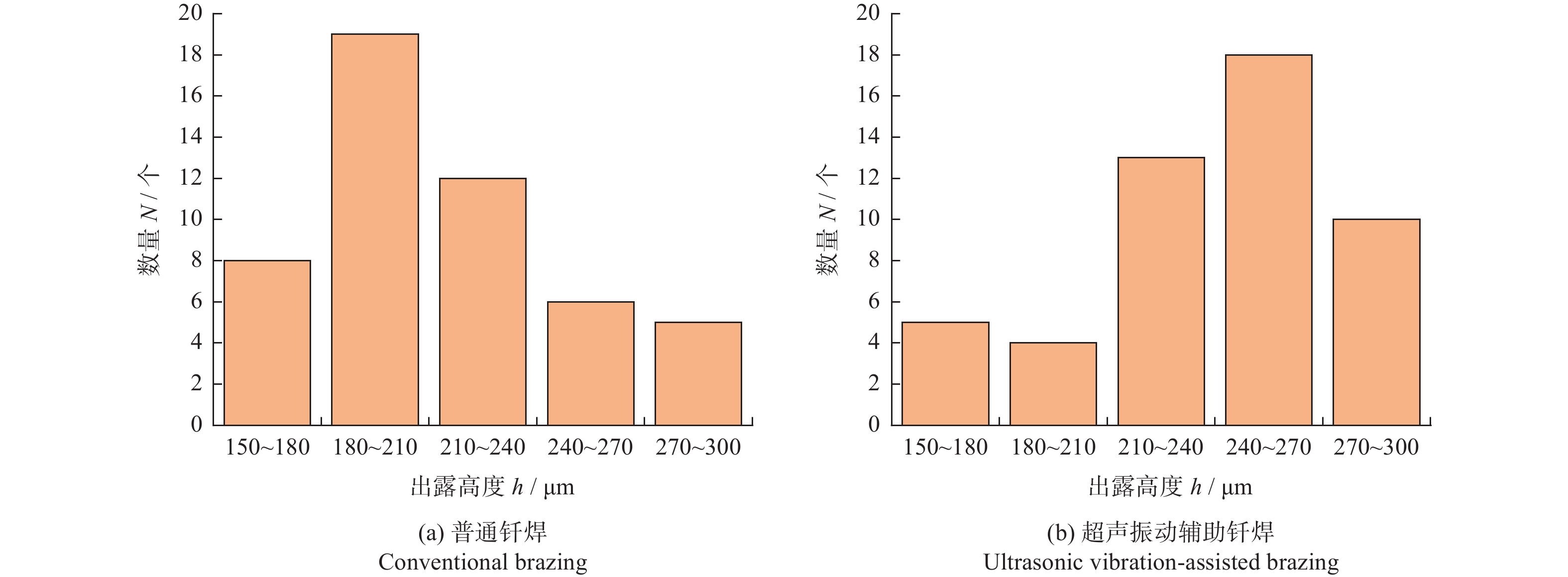
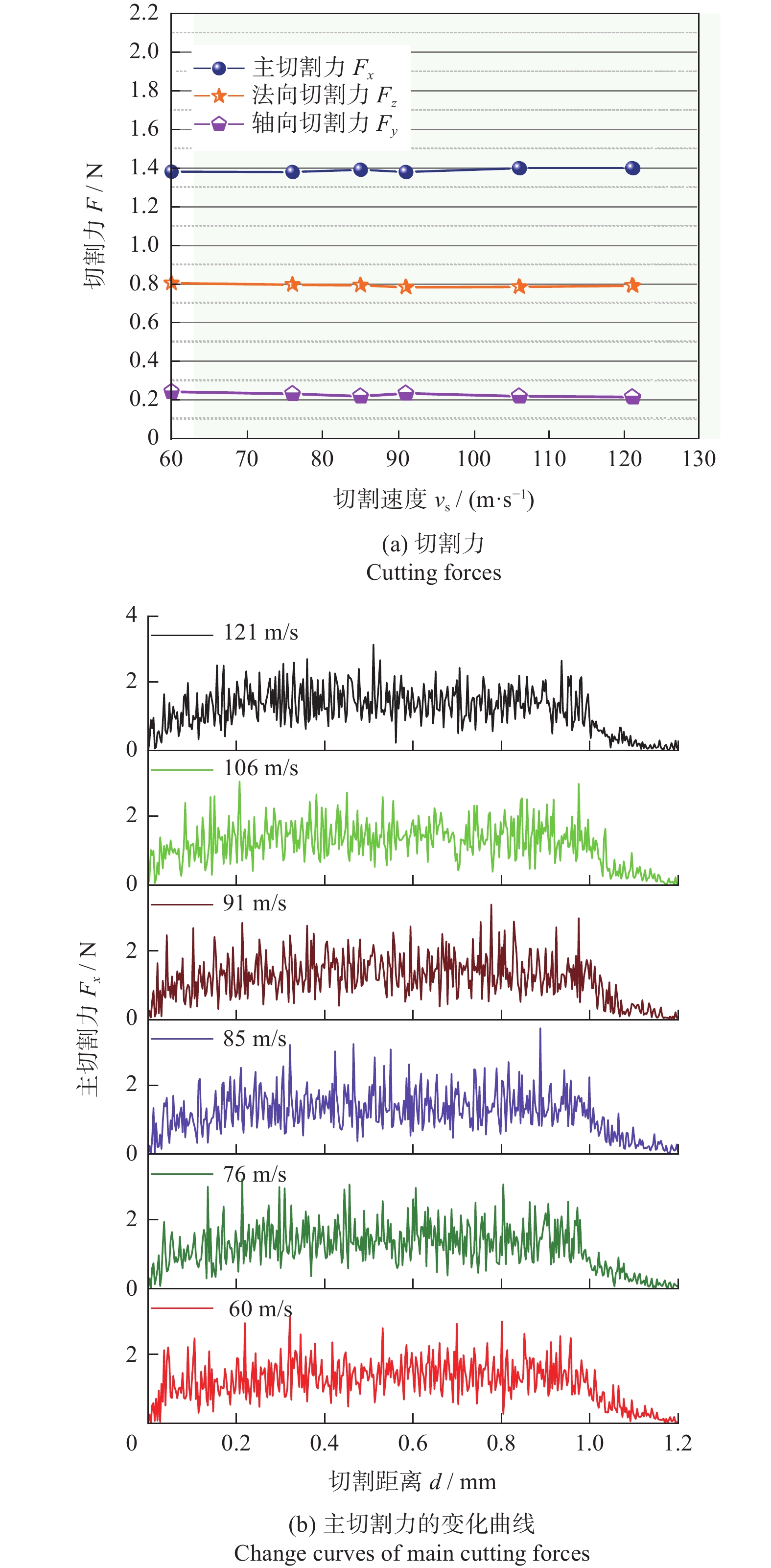
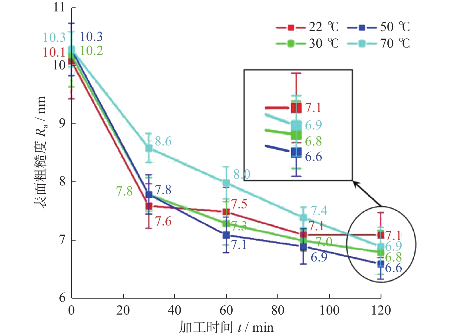
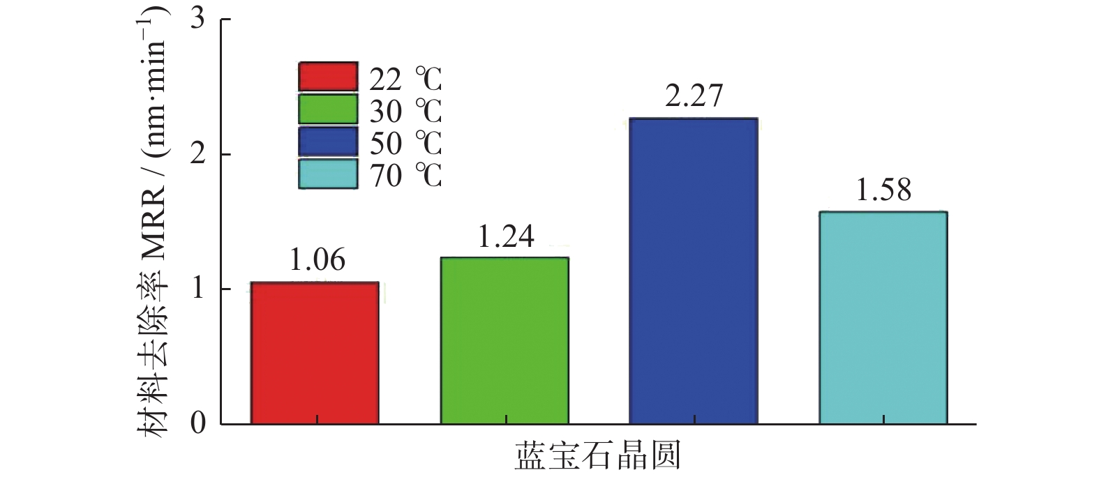
[Objective] Diamond films have been widely used in many fields such as semiconductor devices, optical windows, biomedical applications, heat sink, and mechanical tooling. High quality diamond films need be completely peeled off from the substrate surface for subsequent processing. However, there are still significant challenges in achieving the complete detachment of films. In this paper, a free-standing ultra-thin diamond film with a thickness of about 10 μm and high purity was fabricated using the microwave plasma chemical vapor deposition (MPCVD) method on a glass carbon substrate.
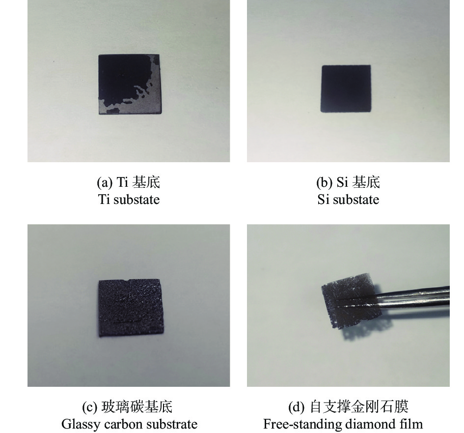
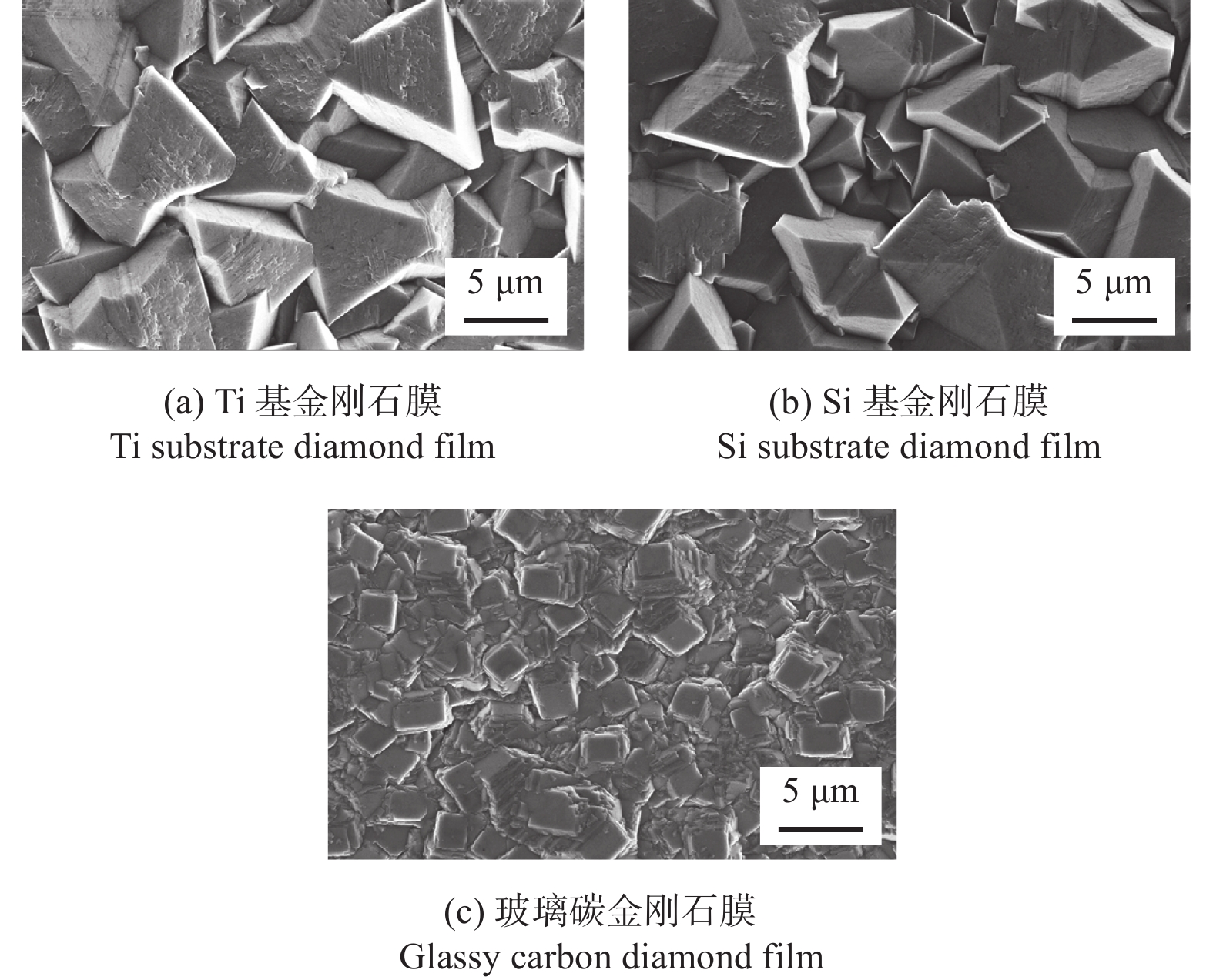
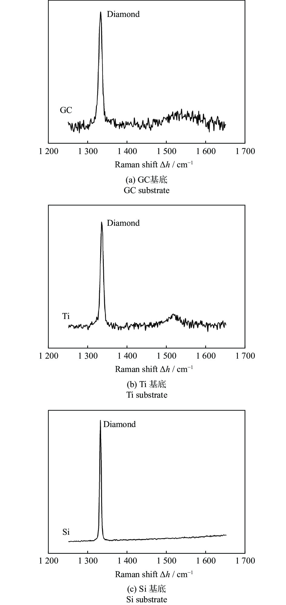
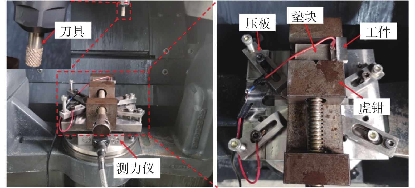
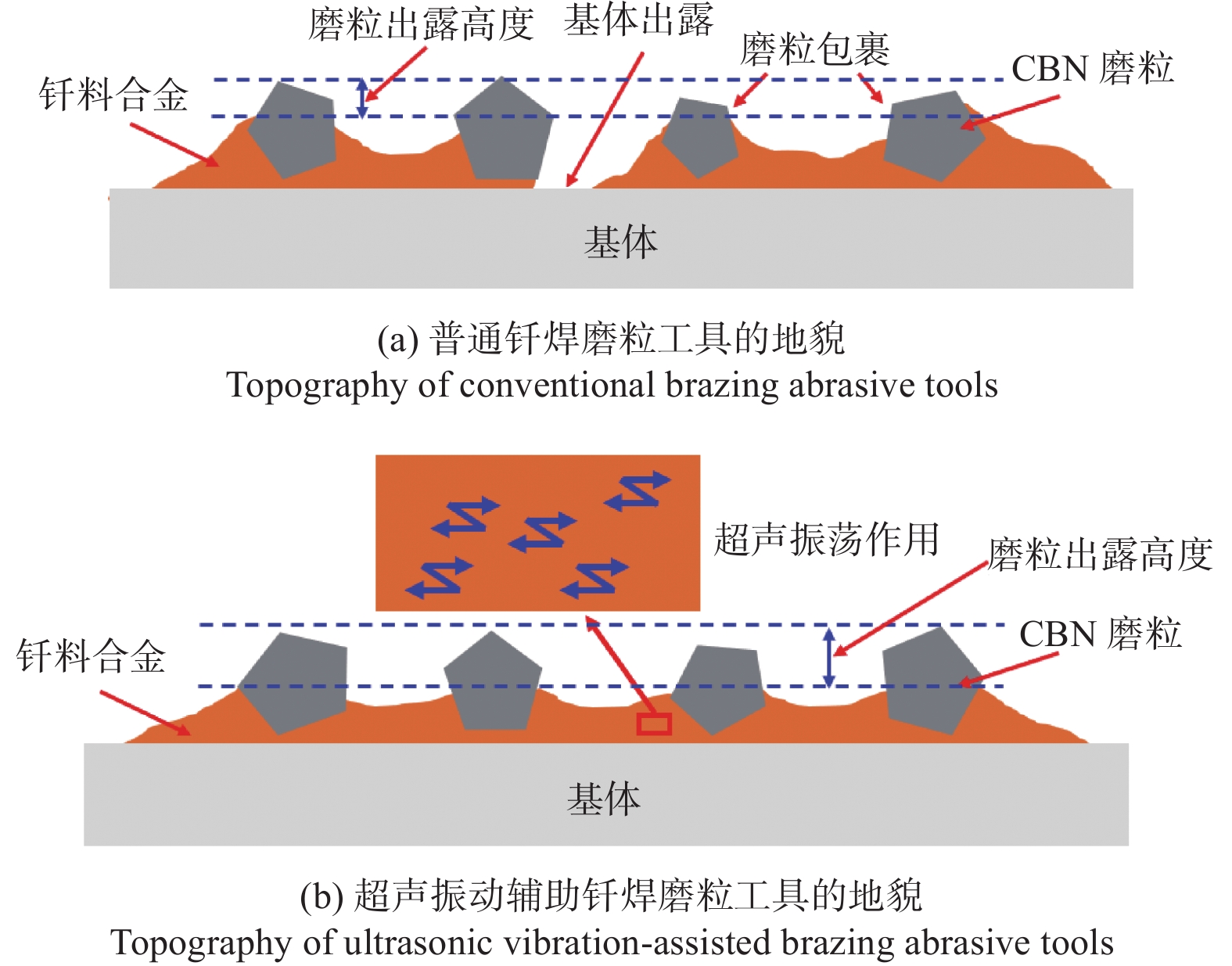
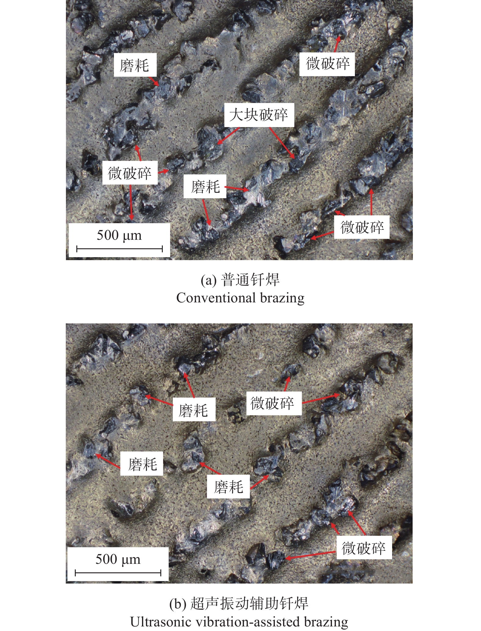
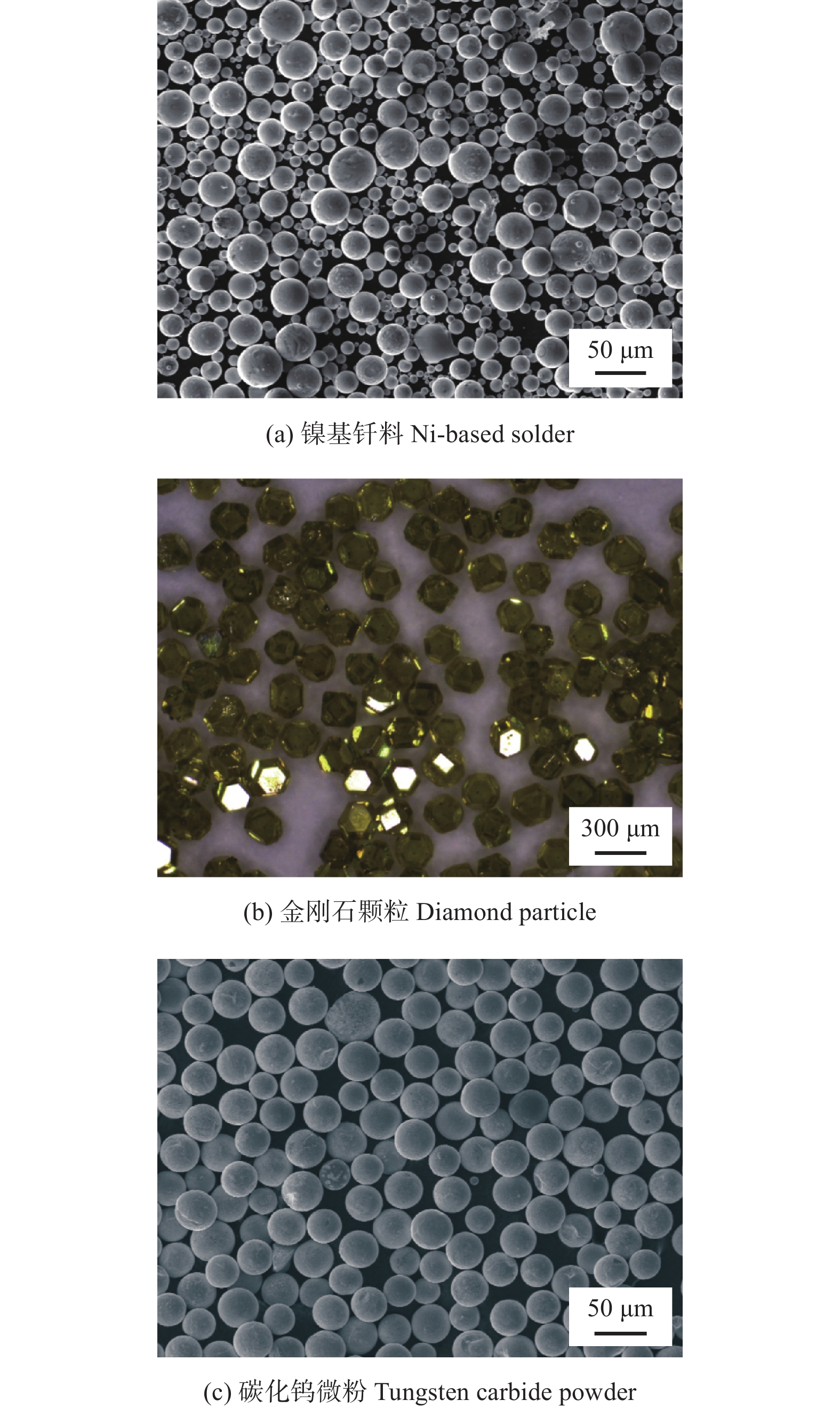
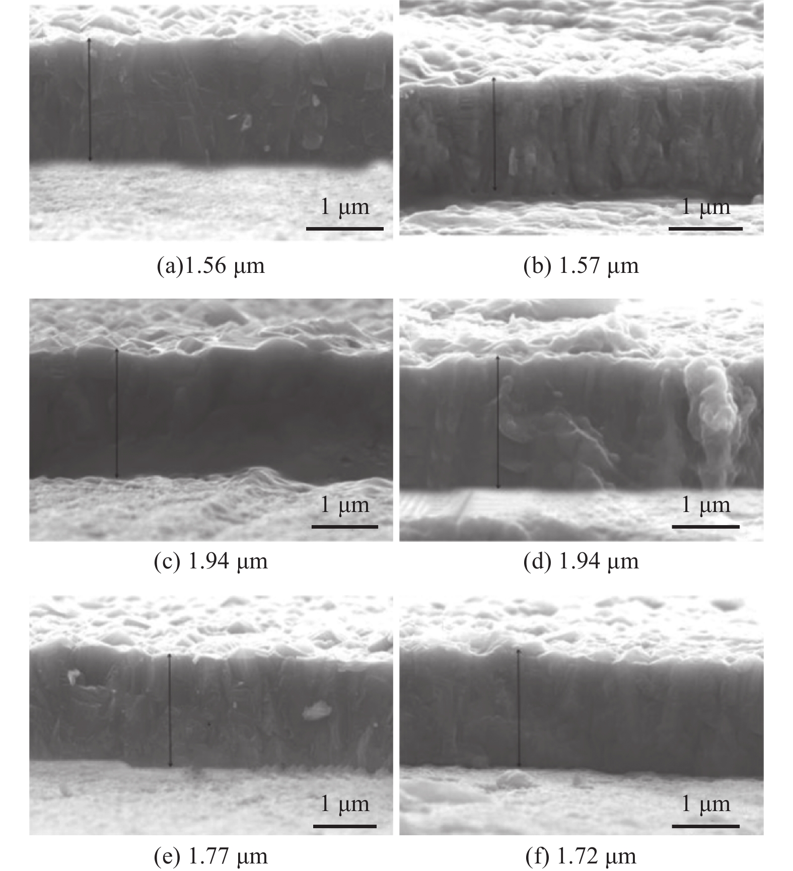
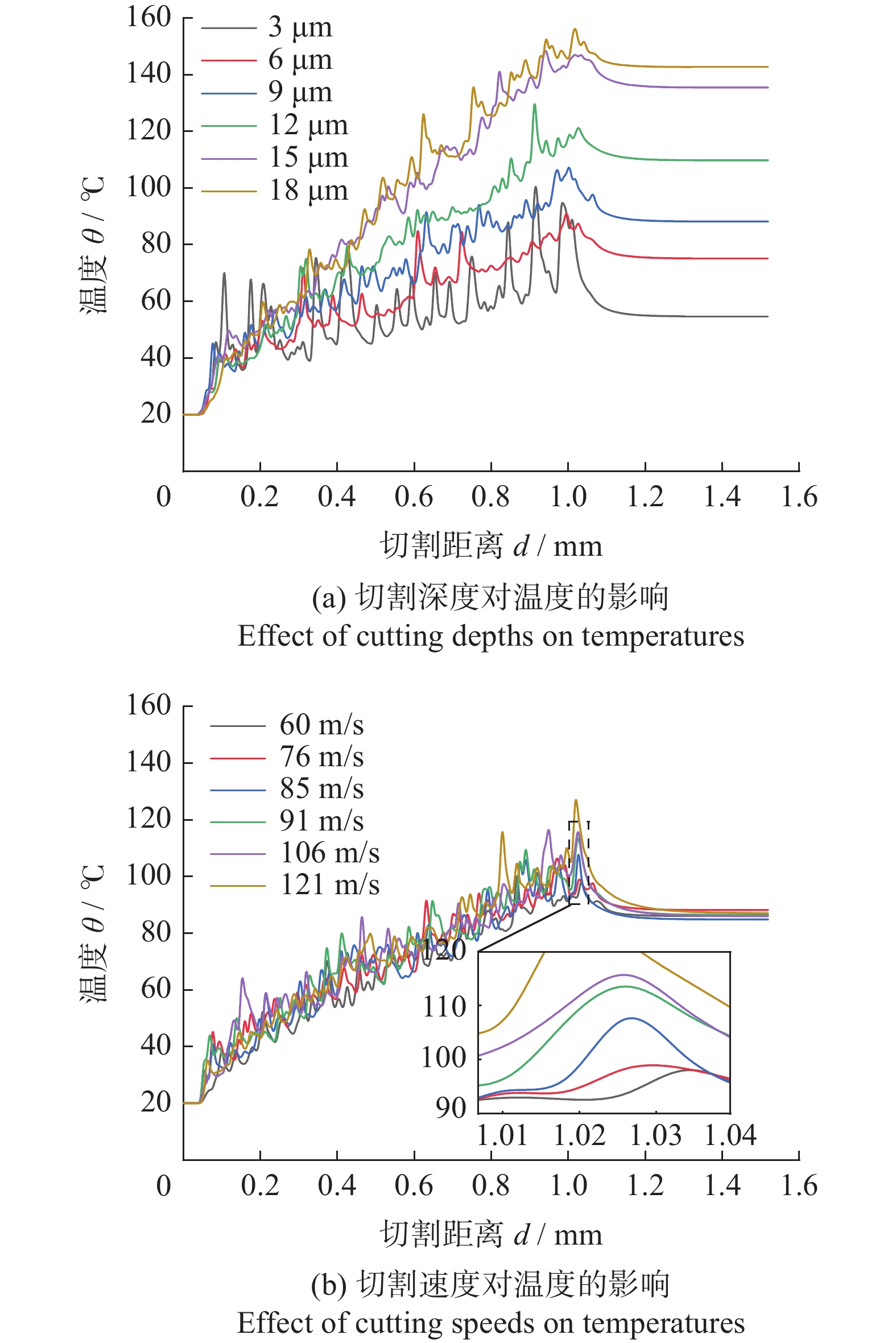
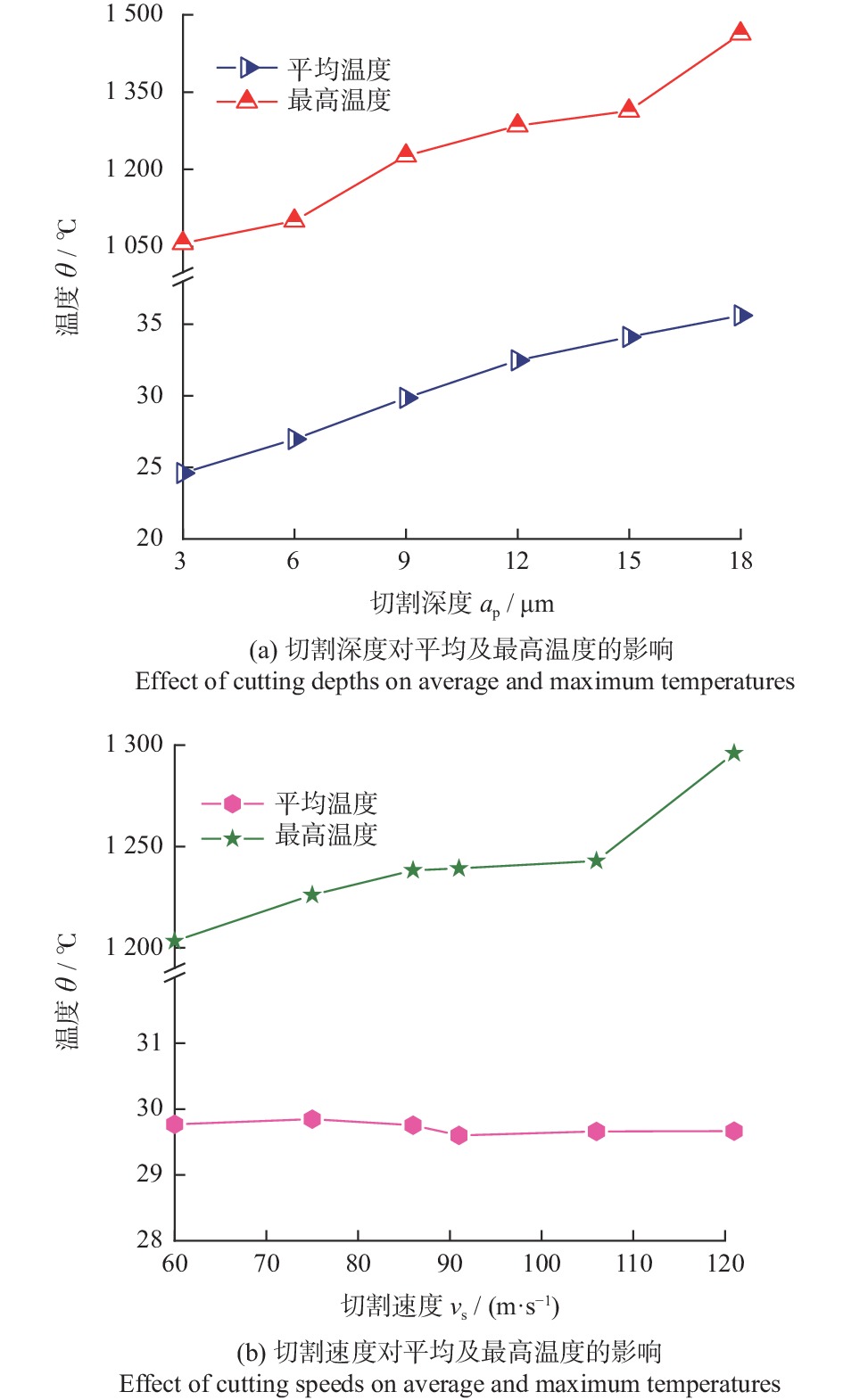
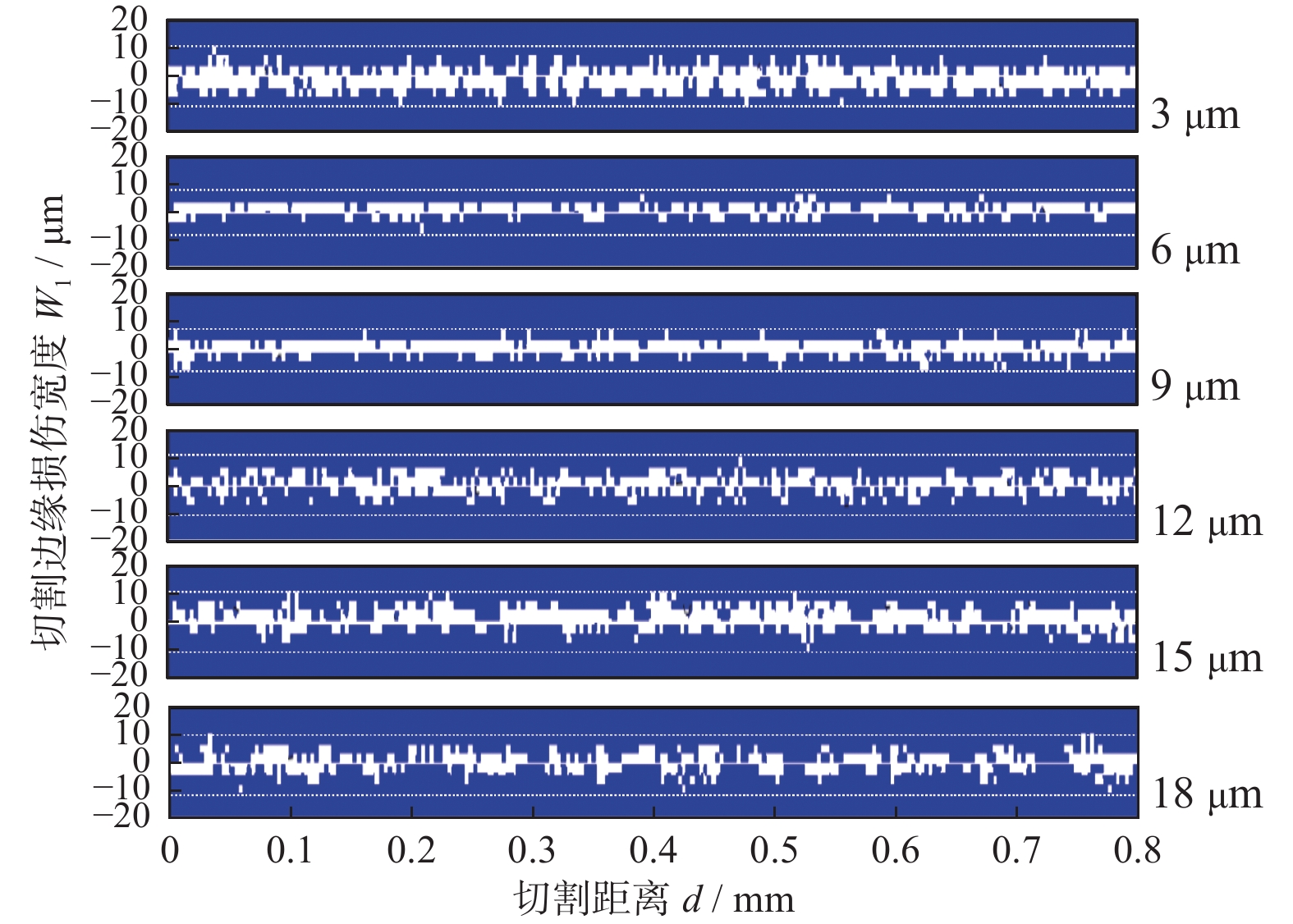
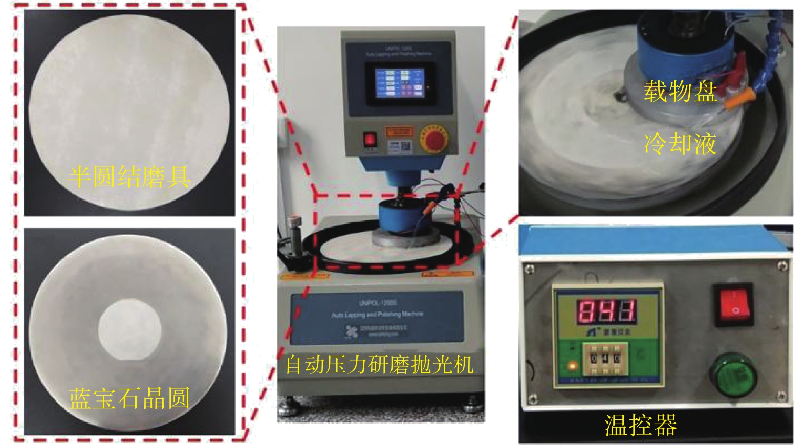
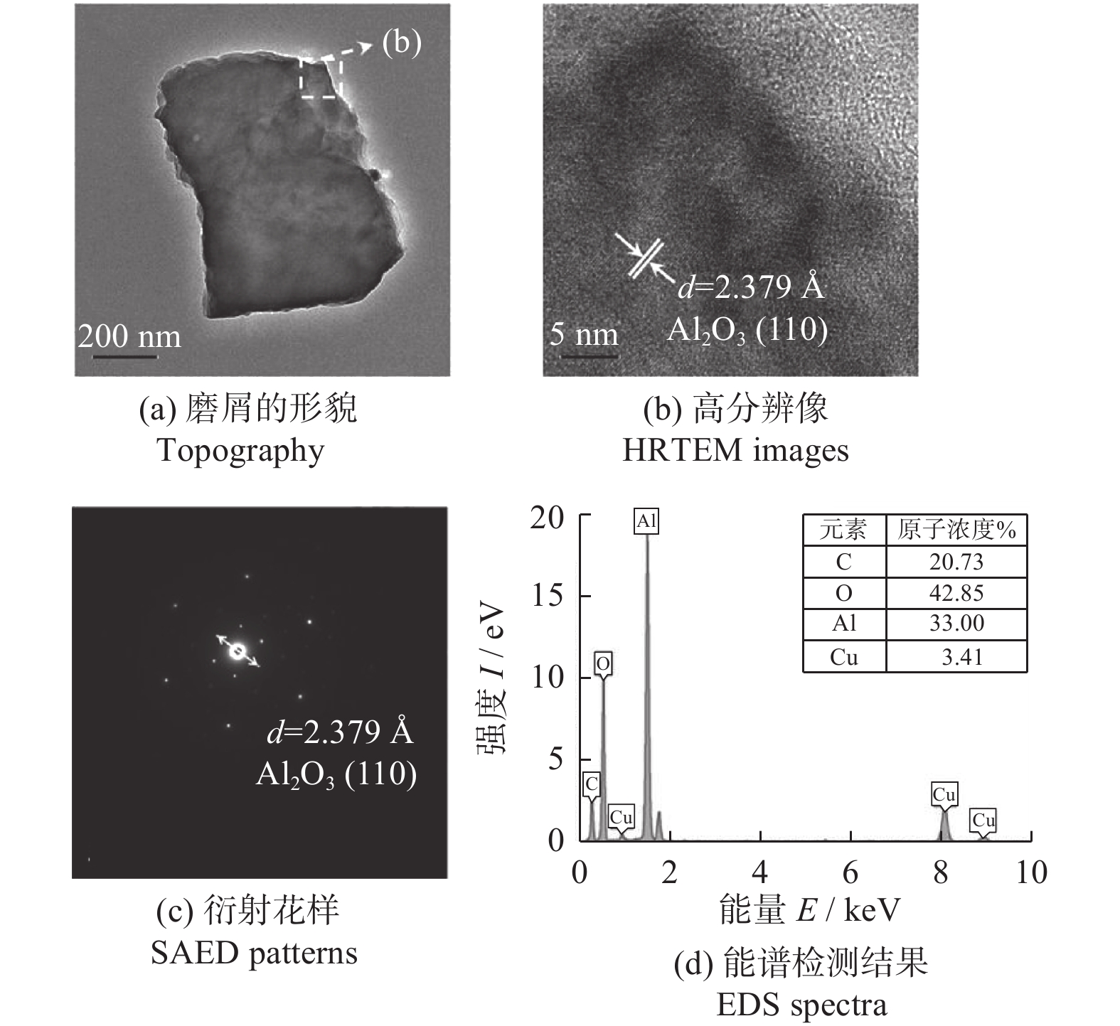
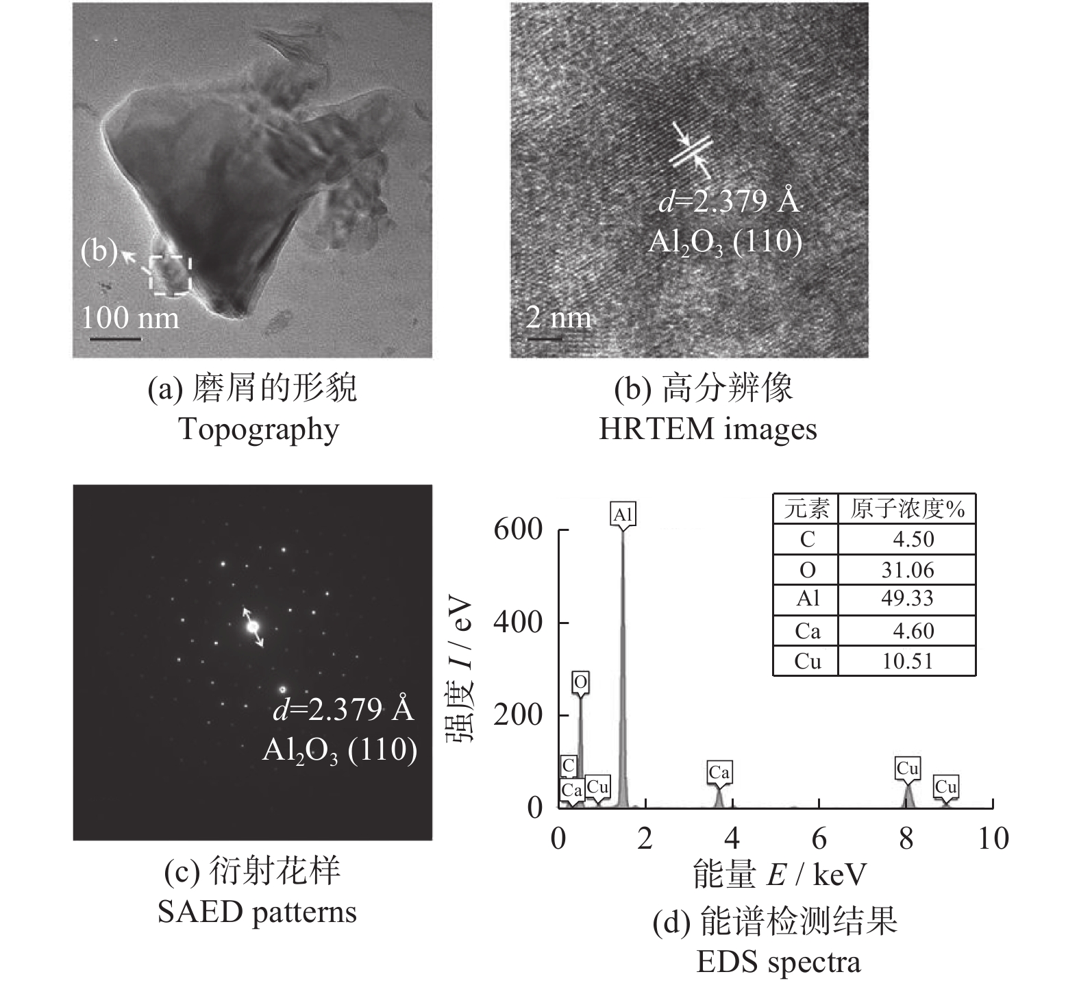
[Method] Three types of substrates, namely titanium (Ti), silicon (Si) and glass carbon, were selected for the fabrication of ultra-thin polycrystalline diamond films using MPCVD with a CH4-H2 mixture as the precursor. The pretreatment for nucleation involved mechanical polishing, followed by ultrasonic vibration-assisted machining with a suspension of diamond microns. The pre-treated substrates were thoroughly cleaned and placed in the MPCVD deposition chamber for growing diamond films under the following conditions: microwave power 5.4 kW, hydrogen (99.99999%) flow rate of 200 sccm, methane (99.99999%) flow rate of 10 sccm, substrate temperature of 870 ℃, chamber pressure of 17.5 kPa, and deposition time of 180 min. SEM, Raman spectrometer and surface profilometer were used to the characterize the overall morphology, surface and cross-sectional surface topography, phase composition, and stresses of the thin diamond films deposited on the three different substrates.
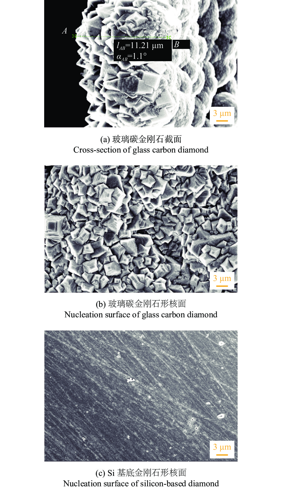
[Results] It was found that the ultra-thin free-standing diamond films grown on the glass carbon substrates were relatively intact with a smooth surface and minimal warping. SEM images revealed that the crystal shapes of all the three diamond films were distinct with tightly bonded grains. The surface topography of the films grown on Ti and Si substrates was similar, both with octahedral surface grains and (111) preferentially oriented crystal plane. In contrast, the grains of diamond films grown on glass carbon substrate (GCD) were mainly cubic, showing a preferential orientation along the (100) crystal plane. Raman spectra of diamond films on different substrates showed strong and sharp characteristic peaks of diamond, indicating high purity and complete crystal structures in all three films. Further analysis of the shift (Δh) between intrinsic peak and characterized Raman peaks revealed that the residual stress in GCD was minimal and predominantly compressive, effectively preventing the occurrence of cracks or fractures in the film and ensuring the integrity of the free-standing films. Conversely, Ti-based diamond films experienced the largest residual stress due to significant differences in their thermal expansion coefficients, which inevitably ld to larger thermal stresses between the diamond film and Ti substrate during cooling. Glassy carbon and diamond had similar thermal expansion coefficients, resulting in smaller thermal stresses during cooling, which was beneficial for the integrity of the free-standing film.
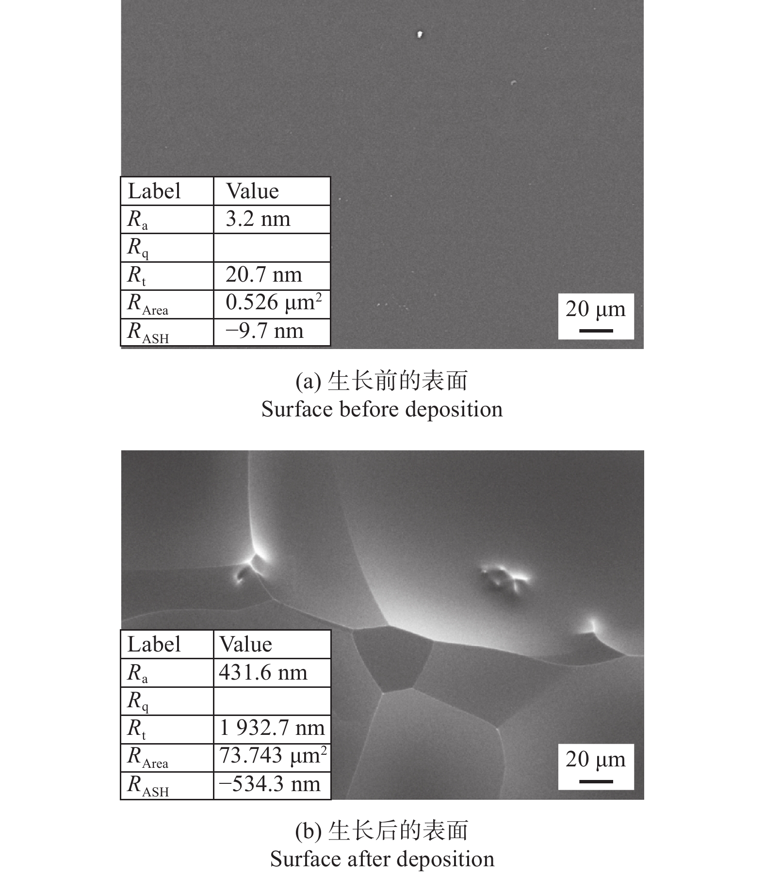
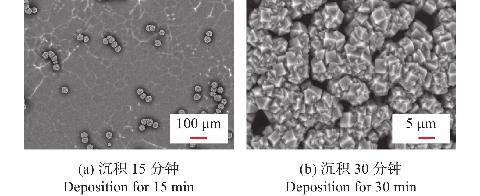
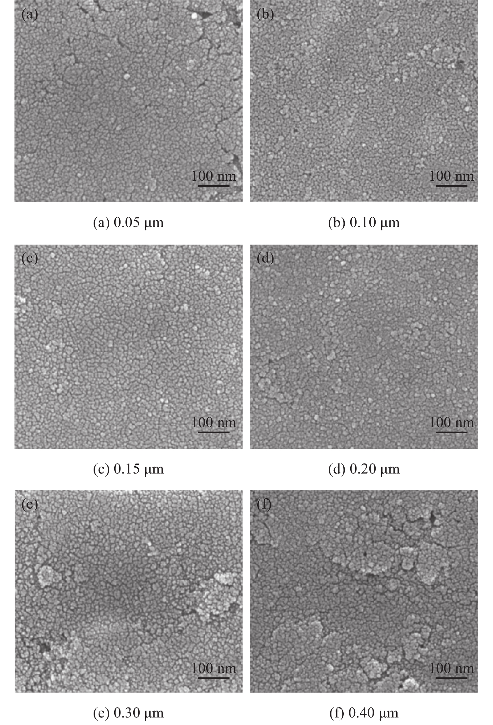
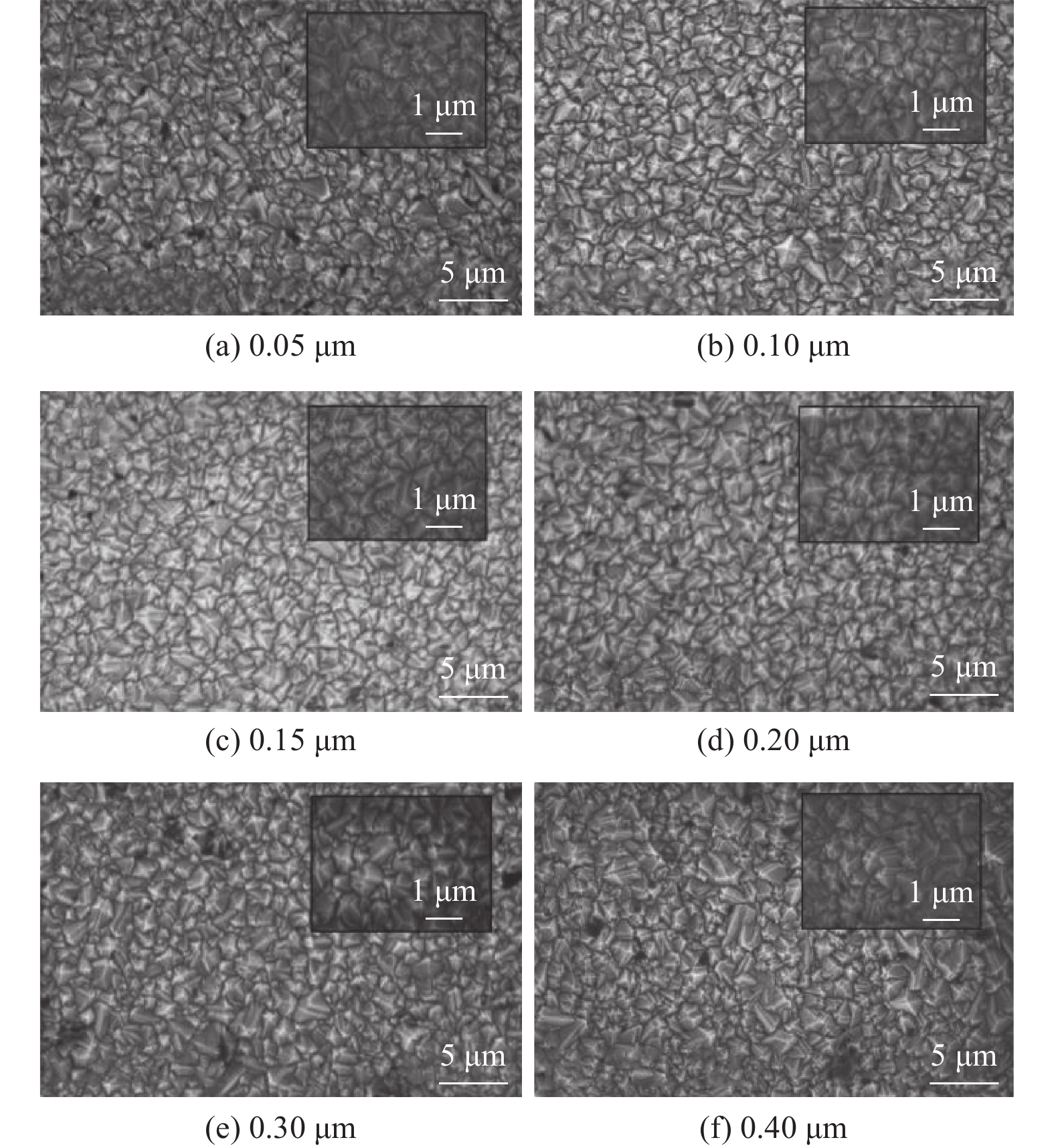
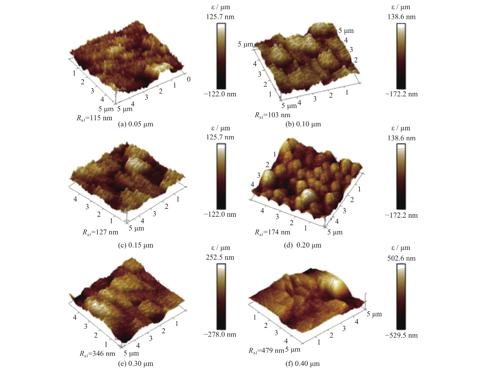
SEM images of the glassy carbon substrate surface before and after growth showed that the surface of the glassy carbon substrate was originally smooth and flat, with a surface roughness of Ra=3.2 nm as measured by a step profiler. Due to the etching effect of H plasma on non-diamond carbon, sand dune-like undulations appeared on the surface of the glassy carbon after the film growth, with a surface roughness of Ra=431.6 nm. This surface morphology weakened the interfacial bonding strength between the diamond film and the substrate, creating a gap between the film material and the substrate. Moreover, as the glassy carbon substrate continued to be etched during the deposition process and the gap widened, the bonding strength at the film-substrate interface would be further weakened. From the SEM images of the substrate surface at different depositing times in the early stages of growth, it was inferred that the process of growing free-standing diamond films on glassy carbon substrates proceeded as follows: during the nucleation stage, carbon-containing precursors formed island-like nuclei on the substrate surface, while the glassy carbon substrate surface was exposed to an H plasma atmosphere and etched into sand dunes. The island-like nuclei then grew into a complete diamond film through an island growth mode.
[Conclusion] Glassy carbon can be effectively used as a substrate to prepare ultra-thin, high-purity free-standing diamond films with a thickness of approximately 10 μm using the MPCVD method. The mechanism for achieving one-step growth and self-supporting peeling of the ultra-thin diamond film is mainly through the etching of the glassy carbon substrate by hydrogen plasma to weaken the interfacial bonding force, ultimately achieving self-peeling. At the same time, the low residual stress of the film material itself ensures the integrity of the film. Choosing glassy carbon as the substrate represents an effective technical approach for meeting the preparation requirements of ultra-thin free-standing diamond films.
 Abstract
 HTML
HTML PDF 2487KB
 Cited By
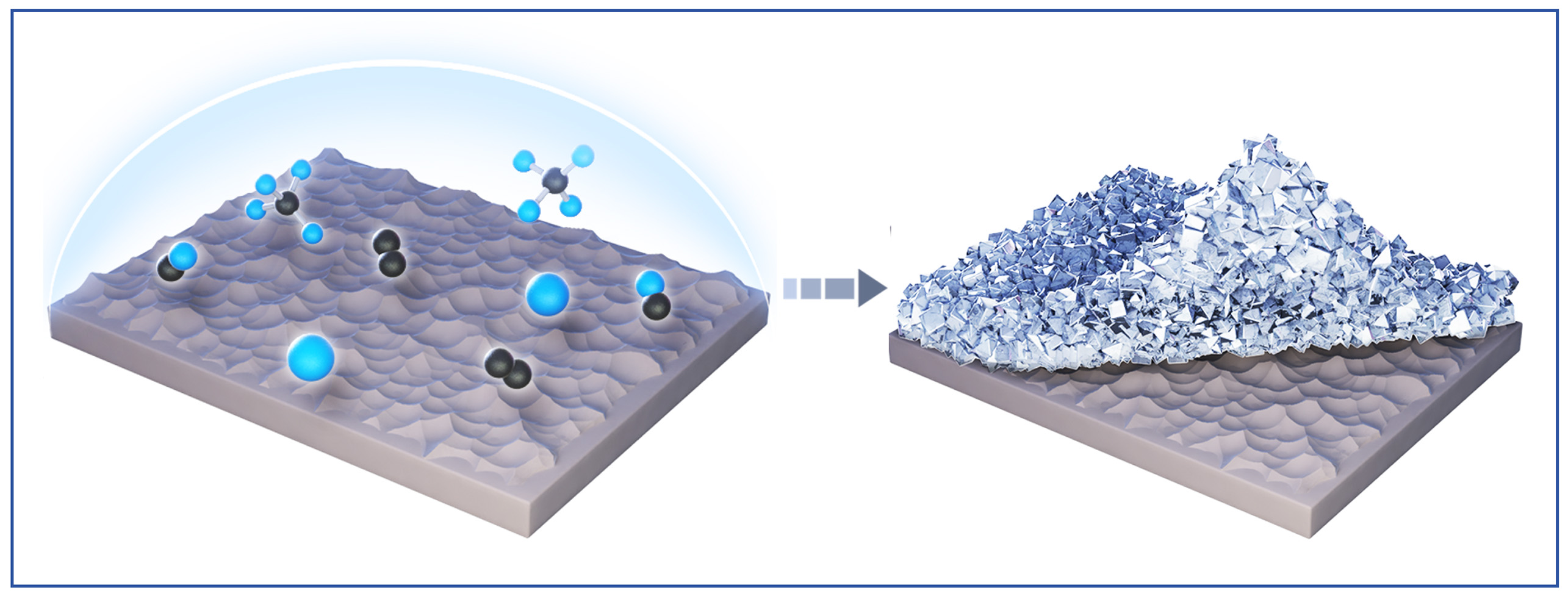


 Email Alerts
 RSS
RSS