Fabrication method of high energy beam for solid-state nanopore
-
摘要: 固态纳米孔因具有机械性能好、稳定性强、形状易控的优点,在基因检测、蛋白质检测、能量转换、物质分离以及水净化等领域显示出巨大的潜力,并引起众多研究人员关注。其中,形状可控、高效的固态纳米孔制造技术是现实固态纳米孔应用的前提。目前,在常见的固态纳米孔制造方法中,高能束制造方法具有高效率、高精度、高可控制造的优势。本文重点概述高能电子束、聚焦离子束、激光刻蚀法和离子径迹刻蚀法等4种固态纳米孔制造方法及其基本原理,并讨论上述方法的优缺点及其大规模可控制造的可行性。Abstract: Solid-state nanopores have drawn the interest of numerous researchers due to their excellent mechanical properties, stability, and shape control, which have demonstrated tremendous potential in gene detection, protein detection, energy conversion, material separation, and water purification. And shape-controlled and efficient solid-state nanopore manufacturing technology is the prerequisite for the application of solid-state nanopore. At present, the high energy beam manufacturing method has the advantages of high efficiency, high precision and high manufacturing controllability among the conventional solid state nanopore manufacturing methods. This paper provides an overview of four solid state nanopore fabrication methods including high energy electron beam, focused ion beam, laser etching and ion track etching and their fundamental principles. The benefits and drawbacks of these methods, as well as their feasibility for large-scale controlled fabrication are discussed.
-
Key words:
- solid nanopore /
- high-energy beam manufacturing /
- manufacturing method.
-
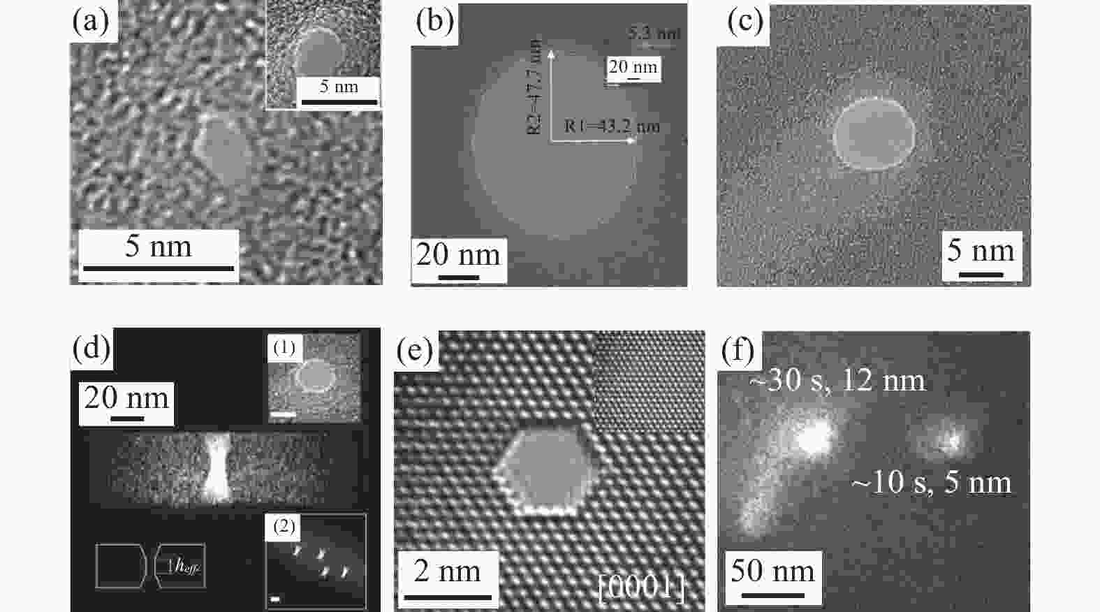
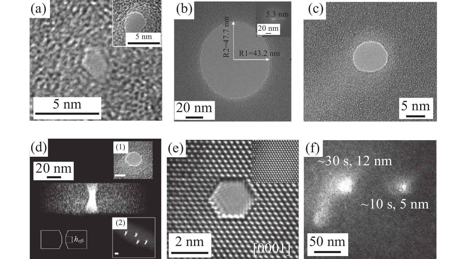
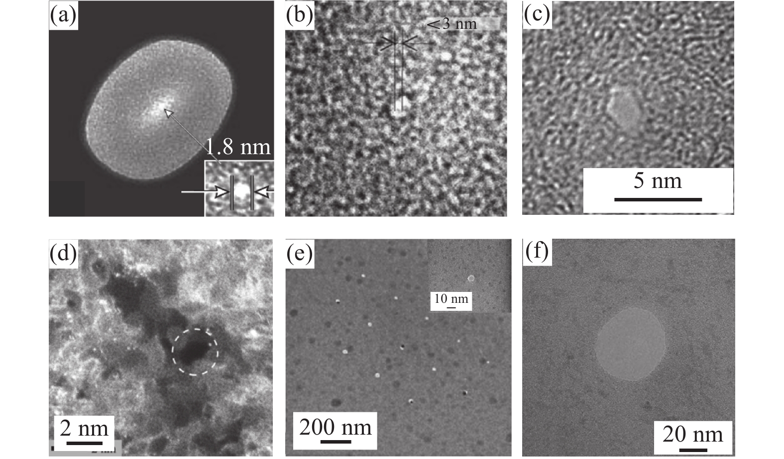
图 3 利用高能电子束制造技术制备的各种固态纳米孔的SEM图和TEM图
(a)利用高能电子束在SiO2薄膜上刻蚀初始直径约为6 nm的纳米孔(右上角插图),后经高强度TEM照射后孔径缩小至2 nm[15];(b)利用FIB制备初始直径约90 nm Si3N4孔,后经SEM辐照将孔缩小至5.3 nm[41](右上角插图);(c)利用聚焦电子束刻蚀得到纳米孔[51];(d)50 nm厚Si3N4膜上直径约7 nm纳米孔的横截面示意图,7 nm孔的俯视图(1),2 nm × 2 nm孔阵列倾斜视图(2)[52];(e)孔径为3.3 nm的Mg纳米孔[47],后在散焦电子束辐照下完全闭合(右上插图);(f)利用SEM制备出孔径小于5 nm的绝缘纳米孔[49]。
Figure 3. SEM and TEM diagrams of various solid nanopores prepared by high-energy electron beam manufacturing technology
(a) A nanopore with an initial diameter of about 6 nm is etched on the SiO2 film by high-energy electron beam (the illustration in the upper right corner), and then the pore size is reduced to 2 nm after high intensity TEM irradiation[15]; (b) The holes with initial diameter of about 45 nm Si3N4 were prepared by FIB, and then the hole was reduced to 5.3 nm [41] by SEM irradiation (illustration in the upper right corner); (c) Nanoholes are obtained by focused electron beam etching[51]; (d) Cross-sectional diagram of about 7 nm diameter nanopore on 50 nm thick Si3N4 film, top view of 7 nm hole (1), 2 nm× 2 nm inclined view of nanopore array (2)[52]; (e) Mg nanopore with a diameter of 3.3 nm [47] was completely closed under the irradiation of defocused electron beam (upper right illustration); (f) Insulated nanopores with aperture less than 5 nm were prepared by SEM[49].
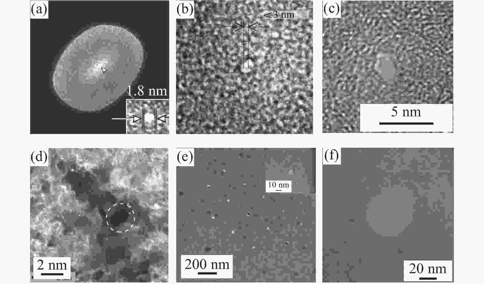
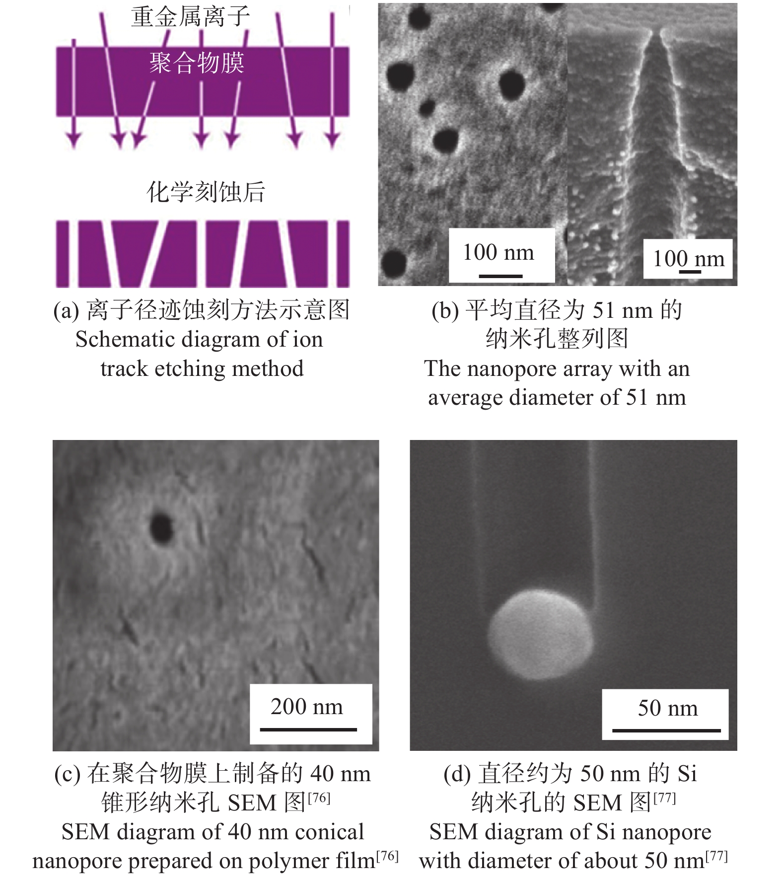
图 4 聚焦离子束制造技术制备的固态纳米孔的SEM和TEM图
(a) Ar + 离子制备Si3N4纳米孔[13]; (b) Ga + 离子制备SiC纳米孔[57];(c)聚焦离子束制备的4 nm Si3N4纳米孔[55];(d) He + 离子制备CNM纳米孔[30];(e)He + 离子制备Si3N4阵列孔和单孔(右上角插图)[65];(f)石墨烯纳米孔[63]。
Figure 4. SEM and TEM images of solid nanopores prepared by focused ion beam manufacturing technology
(a) Preparation of Si3N4 nanopore by Ar + ion[13]; (b) Preparation of SiC nanopore by Ga + ion[57]; (c) 4 nm Si3N4 nanopore prepared by focused ion beam[55]; (d) CNM nanopore prepared by He + ion[30]; (e) Si3N4 array holes and single holes prepared by He + ions (illustration in the upper right corner)[65]; (f) Graphene nanopore[63].
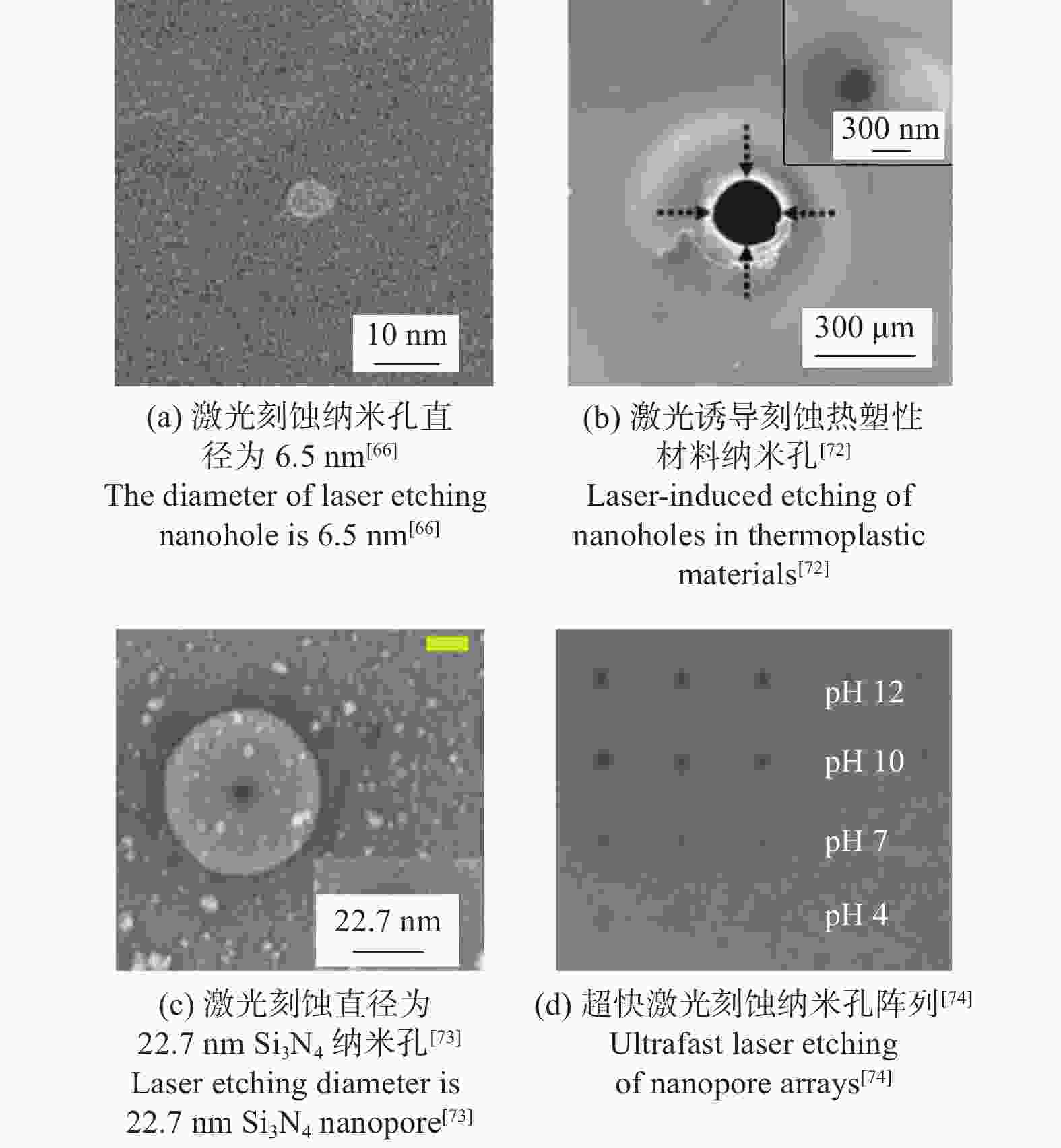
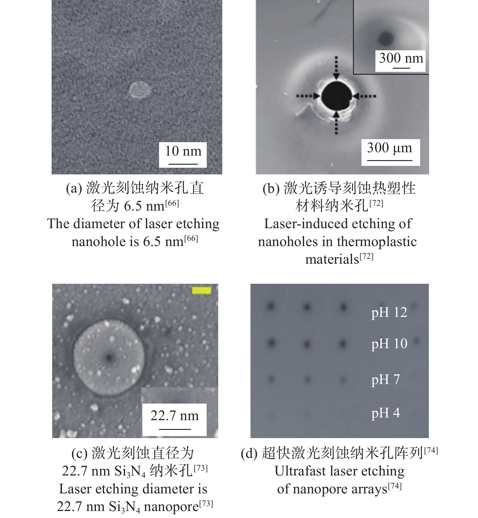
图 5 激光刻蚀技术制备的固态纳米孔的SEM和TEM图
Figure 5. SEM and TEM images of solid-state nanoholes prepared by laser etching technology
表 1 常见的高能束加工固态纳米孔的方法
Table 1. Common methods of machining solid-state nanopores with high-energy beams
 下载: 导出CSV
-
[1] KASIANOWICZ J J, BRANDIN E, BRANTON D, et al. Characterization of individual polynucleotide molecules using a membrane channel [J]. Proceedings of the National Academy of Sciences, 1996,1996,93(24):13770-13773. doi: 10.1073/PNAS.93.24.13770 [2] COULTER W H. Means for counting particles suspended in a fluid: US2656508A [P]. 1953-10-20. [3] KASIANOWICZ J J, ROBERTSON J W, CHAN E R, et al. Nanoscopic porous sensors [J]. Annual Review of Analytical Chemistry,2008,1:737-766. doi: 10.1146/ANNUREV.ANCHEM.1.031207.112818 [4] LI J, STEIN D, MCMULLAN C, et al. Ion-beam sculpting at nanometre length scales [J]. Nature,2001,412(6843):166-169. doi: 10.1038/35084037 [5] JIANG X, ZANG M, LI F, et al. Highly sensitive detection of paraquat with pillar[5]arene as an aptamer in α-hemolysin nanopore [J]. Materials Chemistry Frontiers,2021,5(18):7032-7040. doi: 10.1039/D1QM00875G [6] PAVLENOK M, NIEDERWEIS M. Hetero-oligomeric MspA pores in Mycobacterium smegmatis [J]. Fems Microbiology Letters,2016,363(7):fnw046. doi: 10.1093/femsle/fnw046 [7] HUANG G, VOET A, MAGLIA G. FraC nanopores with adjustable diameter identify the mass of opposite-charge peptides with 44 dalton resolution [J]. Nature Communications,2019,10(1):1-10. doi: 10.1038/s41467-019-08761-6 [8] 段静. MspA蛋白质纳米传感器的制备及其单分子检测应用 [D]. 西安: 西北大学, 2016.DUAN Jing. Preparation and application of the MspA protein nanosensor in single molecule detection [D]. Xi'an: Northwest University, 2016. [9] AKESON M, BRANTON D, KASIANOWICZ J J, et al. Microsecond time-scale discrimination among polycytidylic acid, polyadenylic acid, and polyuridylic acid as homopolymers or as segments within single RNA molecules [J]. Biophysical Journal,1999,77(6):3227-3233. doi: 10.1016/S0006-3495(99)77153-5 [10] ZHANG L, BURNS N, JORDAN M, et al. Macromolecule sensing and tumor biomarker detection by harnessing terminal size and hydrophobicity of viral DNA packaging motor channels into membranes and flow cells [J]. Biomaterials Science,2021,10(1):167-177. doi: 10.1039/D1BM01264A [11] JAIN M, FIDDES I T, MIGA K H, et al. Improved data analysis for the MinION nanopore sequencer [J]. Nature Methods,2015,12(4):351-356. doi: 10.1038/nmeth.3290 [12] VENTA K, SHEMER G, PUSTER M, et al. Differentiation of short, single-stranded DNA homopolymers in solid-state nanopores [J]. ACS Nano,2013,7(5):4629-4636. doi: 10.1021/nn4014388 [13] STORM A J, CHEN J H, LING X S, et al. Fabrication of solid-state nanopores with single-nanometre precision [J]. Nature Materials,2003,2(8):537-540. doi: 10.1038/nmat941 [14] STORM A J, CHEN J H, LING X S, et al. Electron-beam-induced deformations of SiO2 nanostructures [J]. Journal of Applied Physics,2005,98(1):14307. doi: 10.1063/1.1947391 [15] VENKATESAN B M, DORVEL B, YEMENICIOGLU S, et al. Highly sensitive, mechanically stable nanopore sensors for DNA analysis [J]. Advanced Materials,2009,21(27):2771-2776. doi: 10.1002/adma.200803786 [16] GARAJ S, HUBBARD W, REINA A, et al. Graphene as a subnanometre trans-electrode membrane [J]. Nature,2010,467(7312):190-193. doi: 10.1038/NATURE09379 [17] LARKIN J, HENLEY R, BELL D C, et al. Slow DNA transport through nanopores in hafnium oxide membranes [J]. ACS Nano,2013,7(11):10121-10128. doi: 10.1021/nn404326f [18] SHIM J, RIVERA J A, BASHIR R. Electron beam induced local crystallization of HfO2 nanopores for biosensing applications [J]. Nanoscale,2013,5(22):10887-10893. doi: 10.1039/C3NR02608F [19] LIU K, FENG J, KIS A, et al. Atomically thin molybdenum disulfide nanopores with high sensitivity for DNA translocation [J]. ACS Nano,2014,8(3):2504-2511. doi: 10.1021/nn406102h [20] DANDA G, MASIH D P, CHOU Y C, et al. Monolayer WS2 nanopores for DNA translocation with light-adjustable sizes [J]. ACS Nano,2017,11(2):1937-1945. doi: 10.1021/acsnano.6b08028 [21] APEL P. Track etching technique in membrane technology [J]. Radiation Measurements,2001,34(1):559-566. doi: 10.1016/S1350-4487(01)00228-1 [22] DENG Y, HUANG Q, ZHAO Y, et al. Precise fabrication of a 5 nm graphene nanopore with a helium ion microscope for biomolecule detection [J]. Nanotechnology,2017,28(4):045302. doi: 10.1088/1361-6528/28/4/045302 [23] XIA D, HUYNH C, MCVEY S, et al. Rapid fabrication of solid-state nanopores with high reproducibility over a large area using a helium ion microscope [J]. Nanoscale,2018,10(11):5198-5204. doi: 10.1039/C7NR08406D [24] LI W, BELL N A, HERNANDEZ-AINSA S, et al. Single protein molecule detection by glass nanopores [J]. ACS Nano,2013,7(5):4129-4134. doi: 10.1021/nn4004567 [25] SHIM J, KIM Y, HUMPHREYS G I, et al. Nanopore-based assay for detection of methylation in double-stranded DNA fragments [J]. ACS Nano,2015,9(1):290-300. doi: 10.1021/nn5045596 [26] QIU Y. Optimal voltage for nanoparticle detection with thin nanopores [J]. Analyst,2018,143(19):4638-4645. doi: 10.1039/c8an01270a [27] GUO W, CAO L, XIA J, et al. Energy harvesting with single-ion-selective nanopores: A concentration-gradient-driven nanofluidic power source [J]. Advanced Functional Materials,2010,20(8):1339-1344. doi: 10.1002/adfm.200902312 [28] ZHANG W M, WANG Y G, LI J, et al. Controllable shrinking and shaping of silicon nitride nanopores under electron irradiation [J]. Applied Physics Letters,2007,90(16):163102. doi: 10.1063/1.2723680 [29] EMMRICH D, BEYER A, NADZEYKA A, et al. Nanopore fabrication and characterization by helium ion microscopy [J]. Applied Physics Letters,2016,108(16):285310. doi: 10.1063/1.4947277 [30] SIWY Z, FULINSKI A. Fabrication of a synthetic nanopore ion pump [J]. Physical Review Letters,2002,89(19):198103. doi: 10.1103/PhysRevLett.89.198103 [31] KWOK H, BRIGGS K, TABARD-COSSA V. Nanopore fabrication by controlled dielectric breakdown [J]. PLoS One,2014,9(3):e92880. doi: 10.1371/journal.pone.0092880 [32] BELLO J, SHIM J. Solid-state nanopore fabrication in LiCl by controlled dielectric breakdown [J]. Biomed Microdevices,2018,20(2):38. doi: 10.1007/s10544-018-0281-9 [33] YUAN Z, WANG C, YI X, et al. Solid-state nanopore [J]. Nanoscale Research Letters,2018,13(1):56. doi: 10.1186/s11671-018-2463-z [34] LIANG J, CHIK H, YIN A, et al. Two-dimensional lateral superlattices of nanostructures: Nonlithographic formation by anodic membrane template [J]. Journal of Applied Physics,2002,91(4):2544-2546. doi: 10.1063/1.1433173 [35] AYUB M, IVANOV A, HONG J, et al. Precise electrochemical fabrication of sub-20 nm solid-state nanopores for single-molecule biosensing [J]. Journal of Physics: Condensed Matter,2010,22(45):454128. doi: 10.1088/0953-8984/22/45/454128 [36] WU M Y, KRAPF D, ZANDBERGEN M, et al. Formation of nanopores in a SiN/SiO2 membrane with an electron beam [J]. Applied Physics Letters,2005,87(11):113106. doi: 10.1063/1.2043247 [37] SHIN J W, LEE J Y, OH D H, et al. Shrinkage and expansion mechanisms of SiO2 elliptical membrane nanopores [J]. Applied Physics Letters,2008,93(22):221903. doi: 10.1063/1.3027062 [38] KIM M J, WANUNU M, BELL D C, et al. Rapid fabrication of uniformly sized nanopores and nanopore arrays for parallel DNA analysis [J]. Advanced Materials,2006,18(23):3149-3153. doi: 10.1002/ADMA.200601191 [39] CHANG H, IQBAL S M. Fabrication and characterization of solid-state nanopores using a field emission scanning electron microscope [J]. Applied Physics Letters,2006,88(10):103109. doi: 10.1063/1.2179131 [40] YUAN Z, LEI X, WANG C. Controllable fabrication of solid state nanopores array by electron beam shrinking [J]. International Journal of Machine Tools and Manufacture,2020,159(SI):103623. doi: 10.1016/J.IJMACHTOOLS.2020.103623 [41] GOLDSTEIN J I, NEWBURY, D E, ECHLIN P, et al. Scanning electron microscopy and X-ray microanalysis: A text for biologists, materials scientists, and geologists [M]. New York: Springer, 1981. [42] HE K, ROBERTSON A W, GONG C, et al. Controlled formation of closed-edge nanopores in graphene [J]. Nanoscale,2015,7(27):11602-11610. doi: 10.1039/c5nr02277k [43] XU T, XIE X, SUN L. Fabrication of nanopores using electron beam [C]//IEEE Computer Society. The 8th Annual IEEE International Conference on Nano/Micro Engineered and Molecular Systems. Suzhou: IEEE Computer Society, 2013. [44] KIM H M, LEE M H, KIM K B. Theoretical and experimental study of nanopore drilling by a focused electron beam in transmission electron microscopy [J]. Nanotechnology,2011,22(27):275303. doi: 10.1088/0957-4484/22/27/275303 [45] PATTERSON N, ADAMS D P, HODGES V C, et al. Controlled fabrication of nanopores using a direct focused ion beam approach with back face particle detection [J]. Nanotechnology,2008,19(23):235304. doi: 10.1088/0957-4484/19/23/235304 [46] WU S, CAO F, ZHENG H, et al. Fabrication of faceted nanopores in magnesium [J]. Applied Physics Letters,2013,103(24):243101. doi: 10.1063/1.484515 [47] RIGO E, DONG Z, PARK J H, et al. Measurements of the size and correlations between ions using an electrolytic point contact [J]. Nature Communications,2019,10(1):1-13. doi: 10.1038/s41467-019-10265-2 [48] SPINNEY P S, HOWITT D G, SMITH R L, et al. Nanopore formation by low-energy focused electron beam machining [J]. Nanotechnology,2010,21(37):375301. doi: 10.1088/0957-4484/21/37/375301 [49] FISCHBEIN M D, DRNDIĆ M. Sub-10 nm device fabrication in a transmission electron microscope [J]. Nano Letters,2007,7(5):1329-1337. doi: 10.1021/nl0703626 [50] TRAVERSI F, RAILLON C, BENAMEUR S M, et al. Detecting the translocation of DNA through a nanopore using graphene nanoribbons [J]. Nat Nanotechnol,2013,8(12):939-945. doi: 10.1038/nnano.2013.240 [51] STEIN D, LI J, GOLOVCHENKO J A. Ion-beam sculpting time scales [J]. Physical Review Letters,2002,89(27):276106. doi: 10.1103/PhysRevLett.89.276106 [52] HENG J B, HO C, KIM T, et al. Sizing DNA using a nanometer-diameter pore [J]. Biophysical Journal,2004,87(4):2905-2911. doi: 10.1529/biophysj.104.041814 [53] YANG J, FERRANTI D C, STERN L A, et al. Rapid and precise scanning helium ion microscope milling of solid-state nanopores for biomolecule detection [J]. Nanotechnology,2011,22(28):285310. doi: 10.1088/0957-4484/22/28/285310 [54] KUAN A T, GOLOVCHENKO J A. Nanometer-thin solid-state nanopores by cold ion beam sculpting [J]. Applied Physics Letters,2012,100(21):213104. doi: 10.1063/1.4719679 [55] GIERAK J, MADOURI A, BIANCE A, et al. Sub-5 nm FIB direct patterning of nanodevices [J]. Microelectronic Engineering,2007,84(5/6/7/8):779-783. doi: 10.1016/j.mee.2007.01.059 [56] 袁志山. 基于固体纳米孔的 DNA 分子检测器件设计与制造 [D]. 南京: 东南大学, 2016.YUAN Zhishan. Design and fabrication of DNA molecule detection devices based on solid-state nanopores [D]. Nanjing: Southeast University, 2016. [57] 武灵芝, 吴宏文, 刘丽萍, 等. 基于聚焦离子束的氮化硅纳米孔的制备和表征 [J]. 生物物理学报,2013(3):203-212.WU Lingzhi, WU Hongwen, LIU Liping, et al. Fabrication and characterization of solid nanopores with silicon nitride membranes by focus ion beam [J]. Acta Biophysica Sinica,2013(3):203-212. [58] HEMAMOUCHE A, MORIN A, BOURHIS E, et al. FIB patterning of dielectric, metallized and graphene membranes: A comparative study [J]. Microelectronic Engineering,2014,121:87-91. doi: 10.1016/j.mee.2014.03.020 [59] MARSHALL M M, YANG J, HALL A R. Direct and transmission milling of suspended silicon nitride membranes with a focused helium ion beam [J]. Scanning,2012,34(2):101-106. doi: 10.1002/sca.21003 [60] SAWAFTA F, CARLSEN A, HALL A R. Membrane thickness dependence of nanopore formation with a focused helium ion beam [J]. Sensors (Switzerland),2014,14(5):8150-8161. doi: 10.3390/s140508150 [61] 袁志山, 戴敏, 郑李娟, 等. 石墨烯纳米孔传感器制造与单分子过孔形态检测 [J]. 机械工程学报,2022,58(5):190-197. doi: 10.3901/JME.2022.05.190YUAN Zhishan, DAI Min, ZHENG Lijuan, et al. Graphene nanopore sensor fabrication and single molecule translocation form detection [J]. Journal of Mechanical Engineering,2022,58(5):190-197. doi: 10.3901/JME.2022.05.190 [62] HAYASHI T, ARIMA K, YAMASHITA N, et al. Nanopore fabrication of two-dimensional materials on SiO2 membranes using he ion microscopy [J]. IEEE Transactions on Nanotechnology,2018,17(4):727-730. doi: 10.1109/TNANO.2018.2840721 [63] GILBOA T, ZREHEN A, GIRSAULT A, et al. Optically-monitored nanopore fabrication using a focused laser beam [J]. Scientific Reports,2018,8(1):9765. doi: 10.1038/s41598-018-28136-z [64] ZHANG J S K, MIDORIKAWA K. Laser-induced plasmaassisted ablation of fused quartz using the fourth harmonic of a Nd+: YAG laser [J]. Applied Physics A,1998,67:545-549. doi: 10.5772/61567 [65] QIN L, HUANG Y, XIA F, et al. 5 nm nanogap electrodes and arrays by super-resolution laser lithography [J]. Nano Letters,2020,20(7):4916-4923. doi: 10.1021/acs.nanolett.0c00978 [66] GAN Z, CAO Y, EVANS R A, et al. Three-dimensional deep sub-diffraction optical beam lithography with 9 nm feature size [J]. Nature Communication,2013,4:2061. doi: 10.1038/ncomms3061 [67] LIN Z, LIU H, JI L, et al. Realization of approximately 10 nm features on semiconductor surfaces via femtosecond laser direct patterning in far field and in ambient air [J]. Nano Letters,2020,20(7):4947-4952. doi: 10.1021/acs.nanolett.0c01013 [68] LI Z Z, WANG L, FAN H, et al. O-FIB: Far-field-induced near-field breakdown for direct nanowriting in an atmospheric environment [J]. Light Sci Appl,2020,9(1):41. doi: 10.1038/s41377-020-0275-2 [69] WU S, Park S R, LING X S. Lithography-free formation of nanopores in plastic membranes using laser heating [J]. Nano Letters,2006,6(11):2571-2576. doi: 10.1021/nl0619498 [70] LU Y, KAI L, YANG Q, et al. Laser fabrication of nanoholes on silica through surface window assisted nano-drilling (SWAN) [J]. Nanomaterials,2021,11(12):3340. doi: 10.3390/nano11123340 [71] GILBOA T, ZVULONI E, ZREHEN A, et al. Automated, ultra‐fast laser‐drilling of nanometer scale pores and nanopore arrays in aqueous solutions [J]. Advanced Functional Materials,2019,30(18):1900642. doi: 10.1002/adfm.201900642 [72] SIWY Z, DOBREV D, NEUMANN R, et al. Electro-responsive asymmetric nanopores in polyimide with stable ion-current signal [J]. Applied Physics A: Materials Science & Processing,2003,76(5):781-785. doi: 10.1007/s00339-002-1982-7 [73] APEL P Y, KORCHEV Y E, SIWY Z, et al. Diode-like single-ion track membrane prepared by electro-stopping [J]. Nuclear Instruments and Methods in Physics Research (Section B),2001,184(3):337-346. doi: 10.1016/S0168-583X(01)00722-4 [74] SIWY Z S. Ion-current rectification in nanopores and nanotubes with broken symmetry [J]. Advanced Functional Materials,2006,16(6):735-746. doi: 10.1002/adfm.200500471 [75] APEL P Y, BLONSKAYA I V, DMITRIEV S N, et al. Fabrication of nanopores in polymer foils with surfactant-controlled longitudinal profiles [J]. Nanotechnology,2007,18(30):305302. doi: 10.1088/0957-4484/18/30/305302 [76] HARRELL C C, CHOI, Y, HOME L P, et al. Resistive-pulse DNA detection with a conical nanopore sensor [J]. Langmuir,2006,22(25):10837-10843. doi: 10.1021/la061234k [77] TSUJINO K, MATSUMURA M. Morphology of nanoholes formed in silicon by wet etching in solutions containing HF and H2O2 at different concentrations using silver nanoparticles as catalysts [J]. Electrochimica Acta,2007,53(1):28-34. doi: 10.1016/j.electacta.2007.01.035 -

 下载:
下载:


 点击查看大图
计量
- 文章访问数: 1950
- HTML全文浏览量: 877
- PDF下载量: 186
- 被引次数: 0
 邮件订阅
邮件订阅 RSS
RSS